

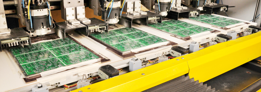
The printed circuit boards are the most common thing in the electronics & the boards are making lives easy by eliminating all the wires & breadboards. Prototyping is one of the ways to get the final copy of the product and thus enables the identification of loopholes in the system. The thorough testing & prototyping will enable the manufacturing of a final product with all the desired features & characteristics.
Before sending the final product to the manufacturer, it is important to catch the flaws & bugs in the design. The printed circuit board prototyping will help in saving valuable time & money in the final production. It works as the proof of concept and ensures demonstration of the product to the investors & consumers. When properly designed, it reduces the size of the device and ensures the final look in the mind of manufacturers.
Let us look at different elements included in the printed circuit boards –
FR4: It is also known as a flame retardant and is a glass-reinforced epoxy resin laminate. It is considered one of the vital parts of the printed circuit boards and also provides a lot of rigidity.
Copper: It is laminated to the board and the process involves adhesive & heat. To determine a one-layer PCB or a multi-layer PCB, it is important to look into the number of copper plates.
Soldermask: It is the layer in place to insulate the copper traces & prevents them from contact with other metals.
Silkscreen: It is the final layer in the printed circuit board and it is used to print letters onto the PCB.
The designing process of electronic products is a complicated one & printed circuit board prototyping is the essential step in the design phase. It has lowered the manufacturing cost & there is no requirement for a complex wiring process. The designers can benefit a lot from the faster turnaround time & the PCB manufacturing process is a tougher one as compared to traditional circuit boards. The lack of wiring makes the PCBs more safe & reliable and is less prone to short-circuits. Also, it prevents the wires from snapping or breaking at any point.
The PCB is mechanically supporting the electronic components like pads, tracks, & other features etched from copper sheets. It has a pre-designed copper track on the conducting sheets & thus reduces the wiring significantly. Thus, the chances of faults arising due to bad connections also decrease significantly. The components need to be placed on the PCB & solder the right way!
The design of PCB is usually done with the conversion of a schematic design into a layout using the right software. Reach out to the right kind of printed circuit board prototyping designer with the right qualities to build to such boards. The prototype will provide the right idea of the circuit board design to the stakeholders. Research before finalizing the prototyping manufacturer for electronic circuit boards.
